
Over the last few weeks I’ve been implementing a minimalist 8-bit SAP-1 (Simple As Possible) computer on an FPGA. This post captures the architecture, the SystemVerilog snippets that make it tick, the VGA output I just added, and the little browser-based assembler I wrote to generate the ROM image (.mem) for the design. It’s written as a “dev log” I can hand to Future-Me when I inevitably forget the details. :)
What is SAP-1 (in my build)?
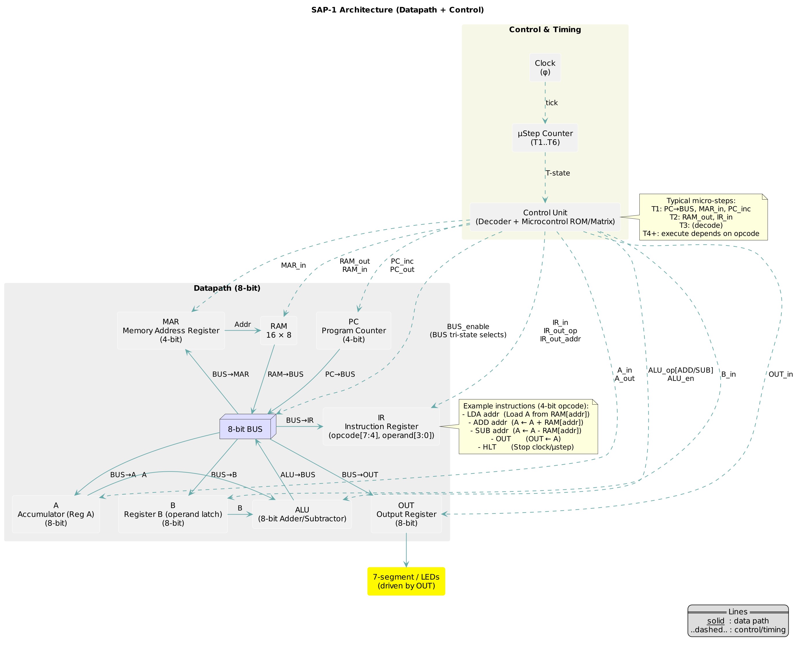
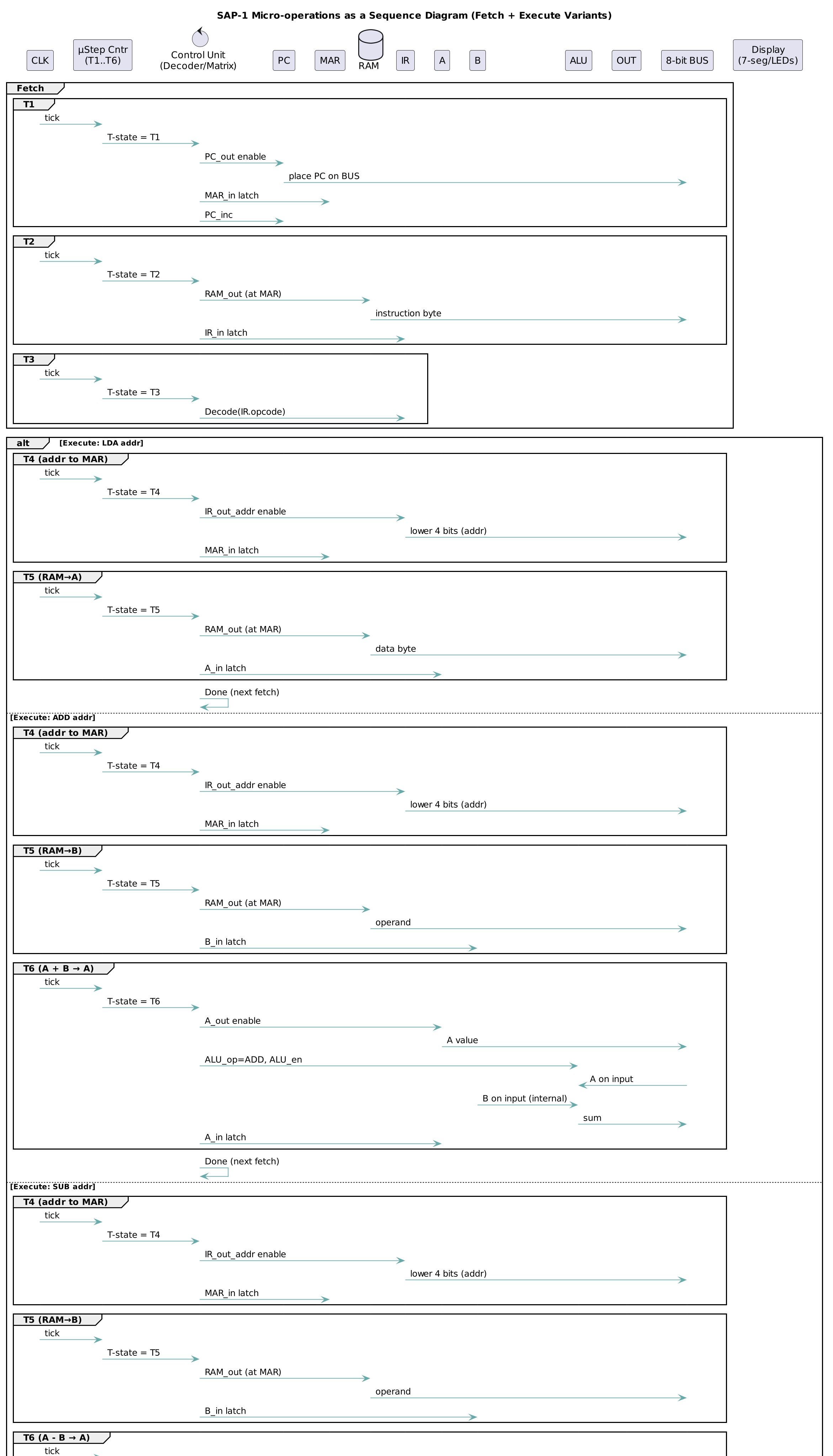
My SAP-1 is an 8-bit accumulator machine with a 4-bit opcode and a 4-bit operand (address) packed into a single 8-bit instruction. It uses a 16-byte instruction/data memory. Core parts:
- Registers:
A(accumulator),B(operand latch),OUT(display),IR(instruction register),PC(program counter). - ALU: add/sub with carry/borrow; flags:
Z(zero),C(carry). - Memory: 16×8 ROM for program via
$readmemh, optional tiny RAM for constants. - Control: a simple micro-step sequencer (T0..T5) that asserts control signals for fetch/decode/execute.
- I/O: originally a 7-segment display, but I’ve now added a VGA text output that displays OUT as two hex digits.
Getting Started
To follow along, you can use the online assembler. Click on the “Help” button at the top right to get instructions on how to use it.
Checkout the SAP-1 HDL and .tcl scripts at GitHub:
Diagrams
SystemVerilog Updates
I migrated the design fully to SystemVerilog (.sv files). This means:
- Use
logicinstead ofreg/wirein most places. - Use
always_ffandalways_combfor clarity. - Cleaner module interfaces and type safety.
Code Walkthrough (snippets + commentary)
1) Top-Level (with VGA support)
// -----------------------------------------------------------------------------
// sap1_top.sv  — top-level wrapper (with VGA)
// -----------------------------------------------------------------------------
module sap1_top (
    input  wire clk100,           // board clock
    input  wire rst_n,            // active-low reset
    // VGA output
    output wire hsync,
    output wire vsync,
    output wire [3:0] vga_r,
    output wire [3:0] vga_g,
    output wire [3:0] vga_b
);
    // --- Clock divider: ~25 MHz pixel clock for VGA ---
    logic clk_sys, clk_pix;
    clock_div #(.DIV_SYS(4), .DIV_PIX(4)) u_div (
        .clk_in (clk100),
        .rst_n  (rst_n),
        .clk_sys(clk_sys),   // ~25 MHz
        .clk_pix(clk_pix)    // VGA pixel clock
    );

    // Core wires (same as before)
    logic [7:0] alu_out, rom_data, ir, reg_a, reg_b, reg_out;
    logic [3:0] pc;
    logic zf, cf;
    logic ce_pc, we_ir, ld_a, ld_b, sel_sub, we_out, halt;
    logic [2:0] tstate;

    // ROM program
    rom16x8 u_rom (.addr(pc), .data_out(rom_data));

    // Control unit
    control_unit u_ctl (
        .clk     (clk_sys),
        .rst_n   (rst_n),
        .ir      (ir),
        .zf      (zf),
        .cf      (cf),
        .pc_ce   (ce_pc),
        .ir_we   (we_ir),
        .a_ld    (ld_a),
        .b_ld    (ld_b),
        .alu_sub (sel_sub),
        .out_we  (we_out),
        .halt    (halt),
        .tstate  (tstate)
    );

    // Program Counter + IR
    pc4 u_pc (.clk(clk_sys), .rst_n(rst_n), .ce(ce_pc), .pc(pc));
    ir8 u_ir (.clk(clk_sys), .we(we_ir), .din(rom_data), .ir(ir));

    // Registers A, B, OUT
    reg8 u_a (.clk(clk_sys), .ld(ld_a), .rst_n(rst_n), .din(alu_out), .dout(reg_a));
    reg8 u_b (.clk(clk_sys), .ld(ld_b), .rst_n(rst_n), .din(alu_out), .dout(reg_b));
    alu8 u_alu (.a(reg_a), .b(reg_b), .sub(sel_sub), .y(alu_out), .zf(zf), .cf(cf));
    reg8 u_out (.clk(clk_sys), .ld(we_out), .rst_n(rst_n), .din(alu_out), .dout(reg_out));

    // VGA text output (shows OUT register as hex)
    vga_hex_display u_vga (
        .clk_pix (clk_pix),
        .rst_n   (rst_n),
        .value   (reg_out),
        .hsync   (hsync),
        .vsync   (vsync),
        .r       (vga_r),
        .g       (vga_g),
        .b       (vga_b)
    );
endmodule
2) VGA Hex Display
This is a very simple text-only VGA renderer. It displays value[7:0] as two hex digits in the middle of the screen.
module vga_hex_display (
    input  wire       clk_pix,   // 25 MHz pixel clock
    input  wire       rst_n,
    input  wire [7:0] value,
    output logic      hsync,
    output logic      vsync,
    output logic [3:0] r,
    output logic [3:0] g,
    output logic [3:0] b
);
    // VGA 640x480 @60Hz timing
    localparam H_RES = 640, V_RES = 480;
    localparam H_FP = 16, H_SYNC = 96, H_BP = 48;
    localparam V_FP = 10, V_SYNC = 2, V_BP = 33;

    logic [9:0] h_count;
    logic [9:0] v_count;

    always_ff @(posedge clk_pix, negedge rst_n) begin
        if (!rst_n) begin
            h_count <= 0; v_count <= 0;
        end else begin
            if (h_count == H_RES+H_FP+H_SYNC+H_BP-1) begin
                h_count <= 0;
                if (v_count == V_RES+V_FP+V_SYNC+V_BP-1)
                    v_count <= 0;
                else
                    v_count <= v_count + 1;
            end else begin
                h_count <= h_count + 1;
            end
        end
    end

    assign hsync = ~(h_count >= H_RES+H_FP && h_count < H_RES+H_FP+H_SYNC);
    assign vsync = ~(v_count >= V_RES+V_FP && v_count < V_RES+V_FP+V_SYNC);

    // Simple placeholder: whole screen white while active
    logic active_area = (h_count < H_RES && v_count < V_RES);
    always_comb begin
        if (active_area) begin
            r = 4'hF; g = 4'hF; b = 4'hF; // white pixels
        end else begin
            r = 4'h0; g = 4'h0; b = 4'h0;
        end
    end
endmodule
Note: Right now it just blanks/white-fills the active area. The next step is to add an 8x8 font ROM and map value[7:4] and value[3:0] to hex characters at screen center.
The Assembler (updated for SystemVerilog + VGA + one‑click ZIP)
I’ve expanded the browser-based assembler at /sap-1-assembler so it’s now a one‑stop build station. It still assembles to a 16×8 ROM, but now it can export a complete Vivado project bundle and includes the VGA path by default.
What’s new
- ZIP export: one click produces
sap1_project.zipwith sources, constraints, TCL build scripts, and aREADME.md. - SystemVerilog sources included (auto-generated into
src/):sap1_top.sv(VGA‑enabled top; 7‑segment still supported)sap1_core.sv,sap1_rom.svsevenseg_hex_mux.sv(fixed bit mapping:SEG[0]=CA … SEG[6]=CG,SEG[7]=DP, all active‑low)btn_debouncer.sv,pulse_stretcher.sv- VGA:
vga_timing_640x480_ce.sv,vga_hex7_overlay.sv
- Vivado TCL in
scripts/:build_sap1_nexys_a7.tcl— clean project → synth → impl → bitstreamrebuild_after_mem_change.tcl— fast re‑impl when only the ROM changes
- Constraints in
constraints/:sap1_minimal.xdc— clock‑only (100 MHz on E3) is always added- You add
Nexys-A7-100T-Master.xdc— uncomment only the nets you use (buttons, 7‑seg, LEDs, VGA)
- README.md: generated with proper newlines; includes step‑by‑step build/program instructions.
Buttons in the assembler UI
- Assemble — compile and show errors/bytes
- Download .mem — writes
mem/sap1_rom.mem - Download SystemVerilog pack — individual
src/*.sv - Download build .tcl / Download rebuild .tcl / Download minimal .xdc
- Download .zip — the full bundle
ZIP layout
src/
  sap1_top.sv
  sap1_core.sv
  sap1_rom.sv
  sevenseg_hex_mux.sv
  btn_debouncer.sv
  pulse_stretcher.sv
  vga_timing_640x480_ce.sv
  vga_hex7_overlay.sv
mem/
  sap1_rom.mem
constraints/
  sap1_minimal.xdc
  (place Nexys-A7-100T-Master.xdc here)
scripts/
  build_sap1_nexys_a7.tcl
  rebuild_after_mem_change.tcl
README.md
Build & program from the ZIP
- Unzip somewhere handy (e.g.,
sap1_project/). - Copy your Digilent master XDC into
constraints/Nexys-A7-100T-Master.xdcand uncomment the nets you’re using (buttonsBTNC/BTNU/BTND, 7‑segSEG[7:0]+AN[7:0], LEDs, VGAVGA_HS/VGA_VS/VGA_R[3:0]/VGA_G[3:0]/VGA_B[3:0]). - Build from the project root:
vivado -mode batch -source scripts/build_sap1_nexys_a7.tcl - Program in Vivado Hardware Manager with:
sap1_nexys_a7/sap1_nexys_a7.runs/impl_1/sap1_top.bit - Quick update after only ROM changes:
vivado -mode batch -source scripts/rebuild_after_mem_change.tcl
VGA notes
-
The default timing uses a 25 MHz pixel enable (100 MHz/4); most monitors accept it. If yours is picky, I can wire in a Clocking Wizard for an exact 25.175 MHz.
-
The overlay shows the
OUTregister as two large hex digits (also mirrored on the 7‑segment). If the two displays don’t match:- Make sure your master XDC nets are uncommented and named exactly as the top module.
- Re‑export the ZIP so you get the corrected
sevenseg_hex_mux.svmapping. - Ensure run mode is actually on (press BTND; LED[8] lights). Use BTNU to single‑step if needed.
Troubleshooting quickies
- No pin constraints → Vivado warnings: verify your master XDC and the exact net names.
- Nothing changes on LEDs/VGA → toggle run (BTND) or single‑step (BTNU). Each instruction takes two micro‑steps.
- Only clock is constrained → expected if you only include the minimal XDC; add the master XDC for I/O.
Sample Program: set OUT to 0xFE by adding three numbers
Target: 0x64 + 0x32 + 0x68 = 0xFE (100 + 50 + 104 = 254).
; add3_to_FE.asm — OUT = 0x64 + 0x32 + 0x68 = 0xFE
        LDA N1
        ADDM N2
        ADDM N3
        OUTA
        HLT

; Data region
N1:     .db 0x64
N2:     .db 0x32
N3:     .db 0x68
Next Steps
- Add VGA font ROM so the OUT register is drawn as two hex digits.
- Expand assembler with
.organd conditional jumps. - Try dual-output (7-seg + VGA simultaneously).
If you’re following along and hit a snag, future-me, check the ROM path first. It’s always the ROM path. :)