SAP-1 on FPGA - Ep. 1
In an effort to better understand computer fundamentals, I have been studying the binary language of 0’s and 1’s. I’m trying to connect the dots between my knowledge of programming languages like C#, C, and the acutal code as it’s executed on the computer hardware.
This led me to the discovery of a great series of videos on making an 8-bit computer on a breadboard by Ben Eater. If you haven’t seen this series of videos and you have an interest in computer hardware, you should definitely check them out.
Ben’s design is based primarily on the SAP-1 (Simple As Possible 1) that was introduced in the book Digital Computer Electronics by Albert Paul Malvino and Jerald A. Brown. I picked up a copy of the book from Thriftbooks (it is out of print). It was relatively inexpensive for a textbook, even one from the 1970’s and 1980’s (mine is a second edition from ~1982).
This post is one in what I hope will be a continuing series (even if it is spread out over years like most of my weekend projects tend to be).
You can follow along on my SAP-1 project on GitHub.
Start at the end
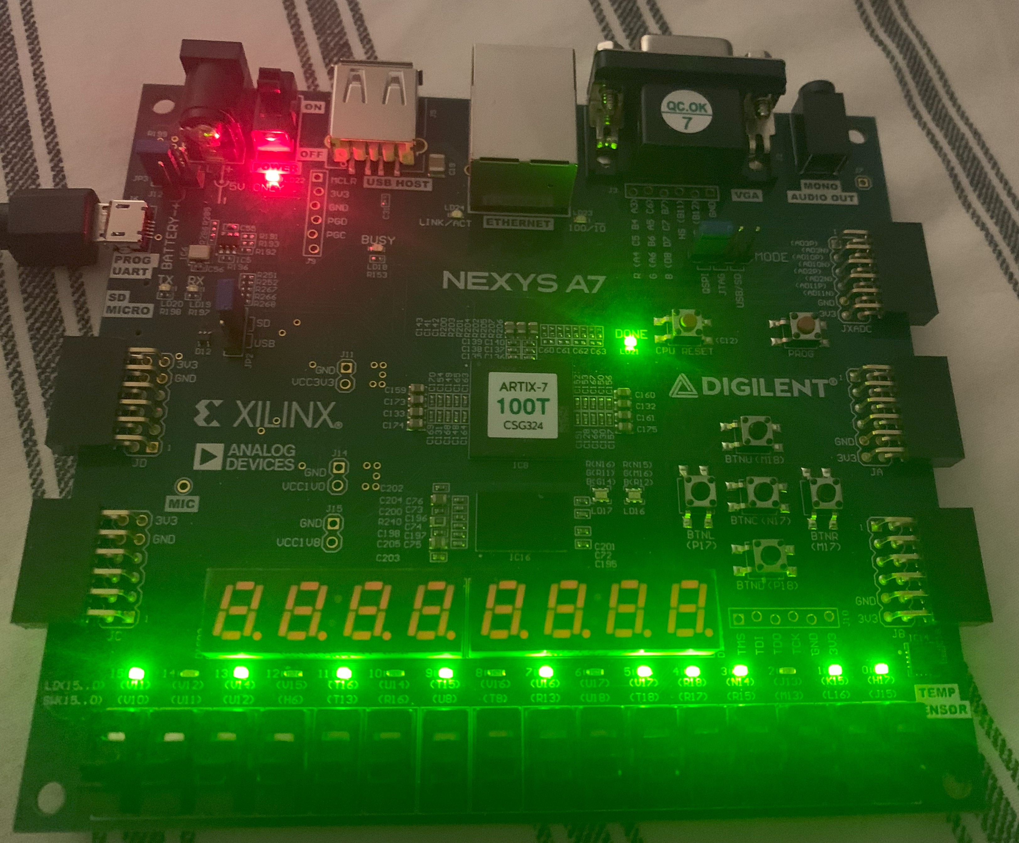
I’ve decided that before I can implement a full computer design in an FPGA, I need to have some sort of output mechanism that lets me see the results of my work as I add more and more modules. I started by building the last piece of the architecture - the 8-bit output display. I am using the Digilent Nexys A7* for my SAP-1 FPGA implementation. It is equipped with 16 LEDs. I decided to make a two-part display, one using the 8 left-most LEDs and one with the 8 right-most LEDs. This will give me two 8-bit displays.
Since I am a pretend Electronics Engineer (after work and on weekends only), I had a lot of trouble getting my head around the 8 digit 7-segment display. I’ll revisit that once I have a little more experience with this implementation. The Nexys board is very new to me, but it looks like it might very well be the best FPGA I have purchased so far and more than powerful enough to implement the SAP-1.
Below is my simple incantation of my LED output circuit.
Verilog
module binary_out(input clk, input [7:0] data1, input [7:0] data2, output reg [15:0] LED);
    reg [15:0] result;

    always @* begin
        result = { data1, data2};
    end

    always @(posedge clk) begin
        LED <= result;
    end
endmodule
For completion, here is the top module that uses it (with some sample data values).
Verilog
module sap_1_top(input CLK100MHZ, output [15:0] LED);
    wire [7:0] data1 = 8'hAA;
    wire [7:0] data2 = 8'hBB;
    binary_out b_out1(clk, data1, data2, LED);
endmodule
Resulting output
Here are the results of the design (please ignore my terrible static electricity prevention protocols).
